[this is a photo, not a graphic representation!]
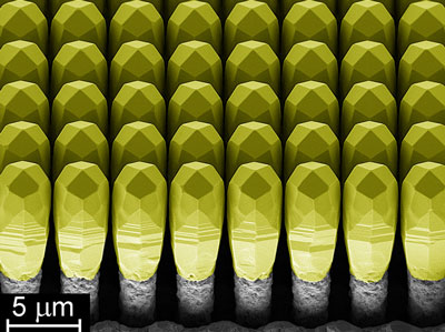
An electron microscope photo of the innovative semiconductor structure: the yellow-coloured heads consist of monolithic germanium and the grey substrate is silicon. (Image: Claudiu Falub, ETH Zurich)
So they are growing these x-photo receptor crystalline arrays in a silicon field~"The elegant alternative of monolithic integration is easily done only if the interatomic spacings and thermal properties of silicon and the combination material differ slightly, or if the layers are comparatively thin", says Professor Hans von Känel, Private Docent at ETH Zurich ... Their paper has just been published in the scientific journal Science ("Scaling Hetero-Epitaxy from Layers to Three-Dimensional Crystals") and is regarded as a breakthrough, which is why it was also chosen as the cover story.
http://www.nanowerk.com/news/newsid=247 ... oo%21+MailThe original aim of the research team's work, which forms part of the Nano-Tera project "NEXRAY" with the CSEM, the EMPA and the ETH as partners, and the CSEM as coordinator, was to produce an X-ray detector grown monolithically on the read-out electronics. The detector needs millions of pixels, which must function simultaneously to guarantee high spatial resolution. A layer of germanium at least 50 microns thick is required to ensure sufficient sensitivity. Large-area detectors produced using previous methods are prohibitively expensive. Hans von Känel stresses that "Our research makes it possible to produce the highest-resolution X-ray detector that has ever existed, and at an affor... allowed germanium crystals to grow on these silicon pillars./quote]
It is also possible to manufacture high-efficiency stacked photovoltaic cells made from semiconductors, with each cell absorbing different wavelengths of sunlight.
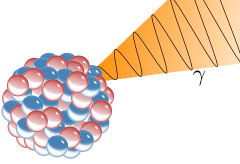
Electricity from x-rays. Wonder what crystal would convert gamma rays ?
The "thermal properties " can probably be described with charge.
s